13 Nov PhD – Charge Trapping in Advanced CMOS Devices at Cryogenic Temperatures for Quantum Computing Applications
Charge Trapping in Advanced CMOS Devices at Cryogenic Temperatures for Quantum Computing Applications
PhD · Leuven · Full time
Unravel fundamental reliability physics to enable large-scale quantum computing
Quantum computing emerges rapidly as a research field that has the potential to push the computational power way beyond the contemporary realm for certain problems. Large-scale quantum computers are not only contenders to break the limits of physical CMOS scaling but have the potential to massively boost fundamental research in various other fields such as chemistry, climate, and computer sciences as well.
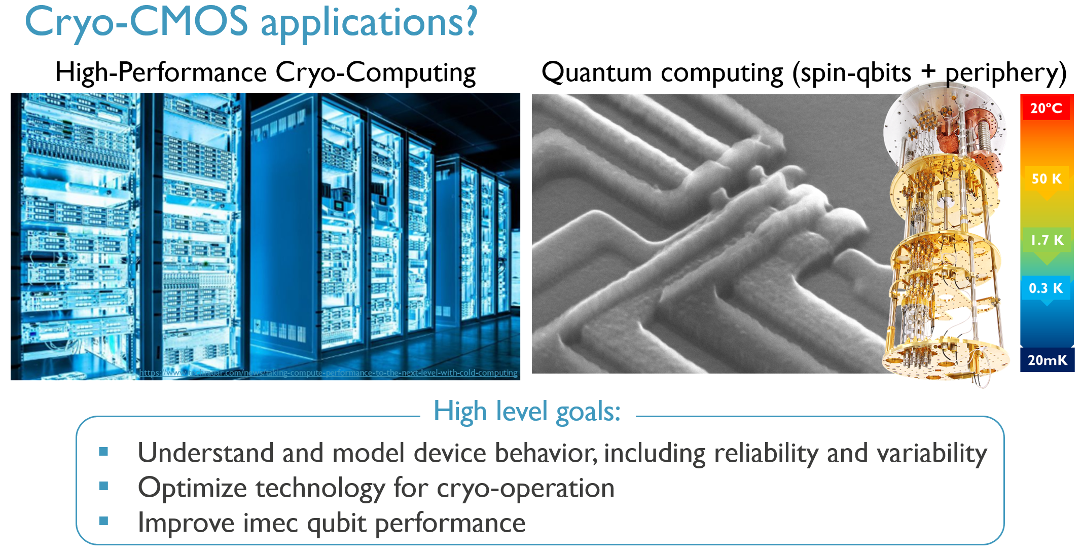
One major hurdle towards large-scale integration is the interface of the qubits to classical control circuitry required to operate them. A promising approach to overcome this problem is to deploy traditional CMOS circuitry in cryogenic environments for efficient operation of future quantum computers.
Traditional reliability models like random telegraph noise, bias temperature instability, and hot-carrier degradation are thought to freeze out at low temperatures. However, recent experimental studies have reported an unexpected weakening of the temperature dependence of charge trapping at cryogenic temperatures, suggesting the need of a fundamental revision and expansion of classical models. On top of that, the fundamental importance of charge noise on the decoherence times of spin-based qubits is creating additional interest for a deeper understanding of charge trapping down to the mK regime.
What you will do:
- You will measure the electrical impact of defect generation and charge trapping in advanced CMOS devices from room-temperature down to cryogenic temperatures
- You will help to mitigate the impact of defects on the operation of spin-qubits and advanced CMOS devices at deep cryogenic temperatures
- Your studies will help to explore the limits of traditional reliability models and improve our understanding of defects in MOS devices at cryogenic temperatures.
Who you are:
- You have a Master’s degree in electrical engineering, microelectronics, physics, or related fields
- You would like to understand and model the physics of defects in MOS stacks at cryogenic temperatures on a fundamental level
- You want to gain hands-on measurement experience in our cryo-lab
- You like to take the initiative; you are persuasive and assured, while keeping a constructive attitude within the team
- Given the international character of imec, a fluent knowledge of English is necessary
References:
- A. Grill et al., IEEE IRPS, 2020, doi: 10.1109/IRPS45951.2020.9128316
- J. Michl et al., IEEE IIEDM, 2021, doi: 10.1109/IEDM19574.2021.9720501
- S. Tyaginov et al., IEEE EDL, vol. 37, 2016, doi: 10.1109/LED.2015.2503920
- A. Beckers et al., IEEE JEDS, vol. 6, 2018, doi: 10.1109/JEDS.2018.2817458
- R. Acharya et al., IEEE VLSI, 2022, doi: 10.1109/VLSITechnologyandCir46769.2022.9830396
Required background: electrical engineering, microelectronics, physics, or related fields
Type of work: 40% electrical characterization of CMOS devices at various temperatures, 40% data analysis and modeling, 20% literature research
Supervisor: Valeri Afanasiev
Co-supervisor: Stanislav Tyaginov
Daily advisor: Alexander Grill, Arnout Beckers
The reference code for this position is 2023-042. Mention this reference code on your application form.
Please click here to apply.
Sorry, the comment form is closed at this time.